Overview
Juicy-footprint is a domain specific language written in/for Java and Scala to design/reconstruct SMD footprints from the Recommended PCB Layout of the datasheet of an SMD component. Recommended PCB Layouts are usually given as engineering drawings where the distances between the parts are relative to each other. Most EDA applications, however, e.g. Eagle, requires SMD footprints to be given in absolute coordinates.
Figuring out absolute coordinates from engineering drawings can be exhausting and error-prone. Juicy-footprint is designed to help with resolving this impedance mismatch. The drawings can be directly represented with the Juicy-footprint DSL, which, when executed, provides absolute coordinates and displays the footprint.
The source code of the library and samples for Java and Scala can be found at https://github.com/domoszlai/juicy-footprint.
How it works
With juicy-footprint one creates shapes and defines relations between their properties (called constraints). The available shapes and their properties are the following:
- Variable: relations can be defined between variables
- Point: x, y: Variable
- HorizontalLine, VerticalLine: p1, p2: Point; length: Variable
- Rect: top, bottom: HorizontalLine; left, right: VerticalLine; width, height: Variable
- Hole: top, bottom, left, right, center: Point; radius: Variable
- Pad: topLeft, topRight, bottomLeft, bottomRight, center, centerTop, centerBottom, centerLeft, centerRight: Point; width, height: Variable
The constraints must be linear, only addition and multiplication with a constant are allowed. The relations between the properties of a shape are pre-defined by the layout engine. So you do not have to tell the engine, e.g., how to calculate the center point from the topLeft and bottomRight coordinates. The library solves the linear equation system defined by the constraints to find absolute coordinates for all the points.
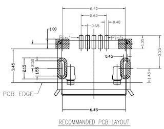
In the following, instead of defining the API dryly, I rather show step-by-syep how to recreate our introductory layout (a micro USB connector) in Scala to get a taste of the library.
A tutorial
The source code of this example can be found at githab.com for Scala and Java.
The very fist thing to do is to instantiate the layout engine that will be used later on to create objects and define constraints:
val l = new Layouter();

Then we can create the first shapes
// 1.5 is a guess, could not find in the spec
val a = l.createPad("A", 1.5, 1);
val b = l.createPad("B", a.width, a.height);
and define their relations:
b.centerTop ~= a.centerTop + (6.4, 0);
Next step, create the five pads for the actual connectors
val p1 = l.createPad("P1", 0.4, 1.35);
val p2 = l.createPad("P2", 0.4, 1.35);
val p3 = l.createPad("P3", 0.4, 1.35);
val p4 = l.createPad("P4", 0.4, 1.35);
val p5 = l.createPad("P5", 0.4, 1.35);
and set their relative positions:
p2.centerTop ~= p3.centerTop - (0.65, 0);
p1.centerTop ~= p2.centerTop - (0.65, 0);
p4.centerTop ~= p3.centerTop + (0.65, 0);
p5.centerTop ~= p4.centerTop + (0.65, 0);
These five pads are nicely placed just in between the two pads on the sides, A and B. It is enough to set a relation between P3 and A and B, the relative positions of the other Ps are already defined.
p3.centerBottom ~= a.centerBottom +
         ((b.centerBottom.x - a.centerBottom.x) / 2, 0);
Create the left pad with the oblong hole (“C.Outside”). The hole is simulated with another pad (“C.Inside”). The constraints are pretty straightforward: (1) their center points are the same (2) the difference between the widths and heights is equal:

val c_inner = l.createPad("C.Inner", 0.45, 1.55);
val c_outer = l.createPad("C.Outer");
c_outer.height ~= 2.15;

c_outer.center ~= c_inner.center; // (1)
c_outer.height - c_inner.height ~=
           c_outer.width - c_inner.width; // (2)
Now the right pad with the oblong hole, the exact same way:
val d_inner = l.createPad("D.Inner", 0.45, 1.55);
val d_outer = l.createPad("D.Outer");
d_outer.height ~= 2.15;

d_outer.center ~= d_inner.center; // (1)
d_outer.height - d_inner.height ~=
           d_outer.width - d_inner.width; // (2)
Still needs to set (1) the relative position of C to D (2) the relative position of C and/or D to the other pads:
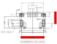
d_inner.center ~= c_inner.center + (6.45, 0); // (1)

// (2)
d_inner.center.y ~= p5.centerTop.y + 3.35;
c_inner.center.y ~= p5.centerTop.y + 3.35;
Horizontally, the distance between A and D (from the left) equals to the distance between B and C (from the right). The A.Center.X and D.Center.X seems different on the layout (also with B and C).
d_outer.centerLeft.x - a.centerLeft.x ~=
               b.centerRight.x - c_outer.centerRight.x;
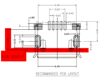
Finally, the PCB edge line is created and positioned:
val edge = l.createHorizontalLine("PCB edge");
edge.p1 ~= a.bottomLeft + (0, 3.45);
edge.length ~= b.bottomRight.x - a.bottomLeft.x;
The very last step is to set an absolute coordinate for any of the points we have (practically the origin):
a.topLeft ~= (0, 0);
From this description, the layout engine is able to derive an absolute coordinate for all the points, and draw the layout:
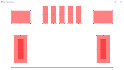
Of course, this is only for convenience and for verifying the result. You are actually interested in the global coordinates calculated by the engine and dumped to the console, so you can easily recreate the PCB layout in e.g. Eagle.
How do you create recommended PCB layouts in your favorite EDA?